VLSI (Very-Large-Scale Integration) has become a game-changer in the fast-paced world of electronics, where performance and efficiency are driven by innovation. It allows engineers to create systems that are small, fast, and energy-efficient by embedding millions of transistors on a single chip. ASIC (Application-Specific Integrated Circuit) design is notable among VLSI applications for its accuracy and adaptability. FITA Academy helps learners build expertise in embedded systems through practical hardware programming and real-world IoT project simulations.
ASICs, in contrast to general-purpose processors, are designed for particular tasks, maximizing efficiency and power consumption. They are essential to modern technology since they power everything from cellphones to artificial intelligence hardware. With an emphasis on ASIC systems, this blog provides a comprehensive guide to learning VLSI design. You will acquire a thorough understanding of design flow, tools, verification, fabrication, and new trends. That characterize the semiconductor business today, regardless of whether you’re a professional honing your craft or a student.
Basics of VLSI and ASIC Design
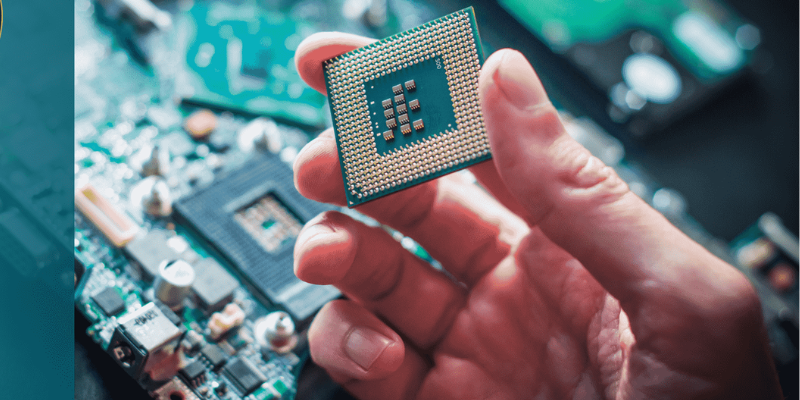
Integrating thousands or millions of electronic components onto a single silicon chip is known as VLSI design. By making gadgets faster, more compact, and more power-efficient, this invention completely changed the electronics sector. The ASIC, a specialized integrated circuit designed to carry out a specific task rather than acting as a general-purpose processor, is at the core of this technology.
An ASIC might only be able to handle data encryption in a security device or signal processing in a smartphone, whereas a CPU can handle a wide range of applications. At massive production sizes, ASICs are optimized for cost, power, and performance. ASICs are faster and more efficient than FPGAs (Field-Programmable Gate Arrays), which may be reconfigured after production. Engineers can better understand why ASICs are the best option for high-volume products that require precision, compactness. Dependability all essential components of contemporary VLSI systems by grasping these fundamental concepts.
How ASIC Systems Power Modern Technology
ASICs are ubiquitous, silently powering the everyday technologies we rely on. They are integrated into IoT devices, data centers, smartphones, and electric cars. All of which carry out specific functions that improve performance. ASICs control power regulation, graphics, and image processing in cellphones. They manage infotainment systems, radar, and sophisticated driver assistance systems in the car industry. Custom ASICs, such as Google’s Tensor Processing Units (TPUs), which are tailored for machine learning and artificial intelligence applications, are also advantageous to the data center sector.
These devices use less energy and do complicated calculations more quickly than conventional CPUs. Beyond commercial applications, ASICs are used in robotics, healthcare, and defense systems. All of which depend heavily on accuracy and efficiency. They are the foundation of next-generation technologies because of their capacity to blend great performance with small size. The need for experts with expertise in VLSI and ASIC design is growing rapidly as industries change. Build your technical expertise by enrolling in the Embedded Course in Chennai . Here you’ll learn microcontroller programming, hardware integration and hands-on embedded project development.
Core Stages of ASIC Design Flow
The ASIC design flow is an organized set of procedures used in ASIC design. Engineers establish the chip’s intended functionality, performance goals, and power requirements at the specification stage. The behavior of the chip is then characterized. Using hardware description languages like Verilog or VHDL during the RTL (Register Transfer Level) design phase.
Before the HDL code is transformed into a gate-level representation during synthesis, the design is simulated to ensure logical soundness. After that, the components are physically positioned and connected on the silicon die during the placement and routing stages of the process. To guarantee peak performance, timing and power analyses are performed on the finished design. Verification and tape-out are the last steps that get the chip ready for manufacturing. To guarantee the ASIC operates dependably during manufacturing. Each stage calls for accuracy, teamwork, and the utilization of specific software tools.
Choosing the Right Design Tools and EDA Software
EDA (Electronic Design Automation) tools, which simplify difficult design and verification activities, are crucial to the success of an ASIC project. Leading companies in the field, such as Cadence, Synopsys, and Mentor Graphics (Siemens EDA), offer cutting-edge platforms for layout design, synthesis, and simulation. For instance, Cadence Virtuoso enables analog and mixed-signal designs, whereas Synopsys Design Compiler assists engineers in converting RTL into efficient gate-level logic. Learners who enroll in an Embedded Training Institute in Chennai build strong hardware and software integration skills, gain expertise in microcontroller programming and real-time systems, and enhance their ability to design innovative embedded solutions for modern devices.
Design rule validation and physical verification are two common uses for Mentor Graphics Calibre. Open-source programs like Magic VLSI, OpenROAD, and GHDL provide accessible learning settings for novices and students. Budget, foundry compatibility, and project complexity all play a role in selecting the appropriate toolkit. To prevent data inconsistencies and delays, engineers must also make sure that tools are properly integrated. Gaining proficiency with EDA software is essential for designers to effectively and precisely manage everything from conceptual modeling to silicon-level optimization.
Designing Efficient RTL and Logic Circuits for ASICs
Data flow and ASIC operations are defined during the RTL (Register Transfer Level) design stage. Engineers specify logical behavior using Verilog or VHDL, emphasizing maintainability, efficiency, and modularity. Performance, power consumption, and verification time can all be greatly impacted by a well-organized RTL architecture. Engineers should use consistent naming standards for clarity and break up complex circuits into smaller, reusable modules in order to design effectively.
To maximize resource use, pipelining, clock gating, and low-power design strategies are crucial. Early and frequent simulation reduces time and expense by identifying logic flaws prior to synthesis. In order to prevent functional mismatches, engineers must also take into account time limitations and guarantee synchronization among modules. By following these guidelines, designers produce ASICs that not only satisfy functional specifications but also offer excellent performance and power efficiency two essential success elements in the cutthroat semiconductor market of today.
Testing and Verification: Ensuring ASIC Reliability
Verification is a crucial stage in ASIC design that guarantees the chip performs as planned in practical settings. Engineers spend a lot of effort on validation using sophisticated verification techniques because manufacturing errors can be expensive. Static timing analysis (STA) is used to verify timing accuracy, formal verification is used for mathematical confirmation of design conformity, and functional simulation is used to assess logical correctness.
In order to evaluate real-world performance, engineers also run post-layout simulations following placement and routing. Automated testbench construction is made possible by verification frameworks such as UVM (Universal Verification Methodology), which increases coverage and decreases manual labor. The comprehensive testing of all design scenarios is further ensured by assertions and coverage measures. An ASIC that has undergone thorough verification reduces the possibility of failure during fabrication, which lowers development time and costs. In addition to ensuring dependability, effective verification techniques boost consumer trust in the functionality and long-term stability of the finished product.
Fabrication and Tape-Out: From Design to Silicon
The ASIC proceeds to the fabrication stage, when digital blueprints are transformed into actual silicon, once the design has been confirmed and approved. Tape-out is the first step in the process, when each circuit layer is represented by a photomask. These masks direct the etching of transistor designs onto silicon wafers via lithography tools. This extremely complex technique is handled by semiconductor foundries like as GlobalFoundries, Samsung Foundry, and TSMC. So this is why Linux is used in embedded system.
Performance, power efficiency, and transistor density are all influenced by the fabrication node selection (e.g., 7nm, 14nm, 28nm). To guarantee that only flawless chips are transported, wafers are tested and packaged after etching. Because even a minor layout error might render an entire batch unusable, this step requires extraordinary care. Timing, power, and area requirements are satisfied when design engineers and fabrication experts work together. The process of fabrication turns abstract concepts into real, high-performing ASICs that may drive cutting-edge technologies.
Challenges and Common Pitfalls in ASIC Design
ASIC design is intricate and fraught with difficulties. One of the main obstacles is high development costs since EDA tool licenses, fabrication, and verification need significant investment. The lengthy design cycle, which frequently takes months because of intensive testing and modeling, is another problem. Power, performance, and area trade-offs (PPA) require ongoing balance because enhancing one factor may have a detrimental impact on another. Since signal propagation delays must adhere to stringent requirements in order to guarantee chip stability, timing closure is another ongoing challenge.
Additionally, troubleshooting later on becomes challenging, highlighting the importance of early error identification. Cost-effectiveness can also be impacted by manufacturing yield, particularly at smaller process nodes. Engineers should use organized workflows, keep thorough records, and embrace automation to avoid these hazards. Reliable, economical, and high-quality ASIC devices are made possible by ongoing learning and cooperation between the design, verification, and manufacturing teams.
Integrating VLSI Design with Emerging Technologies
Neuromorphic computing is also opening the door to new advances in real-time processing and energy-efficient design. These days, engineers combine software-driven optimization and machine learning-based design tools with conventional VLSI techniques. In order to create future semiconductor systems that are quicker, smarter, and more sustainable, VLSI specialists must increase their skill sets when various technologies converge.
Neuromorphic computing, which draws inspiration from the human brain, is also paving the way for new developments in energy-efficient design and real-time processing. These days, engineers combine software-driven optimization and machine learning-based design tools with conventional VLSI techniques. In order to create future semiconductor systems that are quicker, smarter, and more sustainable, VLSI specialists must increase their skill sets when various technologies converge.
Tips for Beginners and Career Opportunities in VLSI Design
Learning VLSI design can lead to fascinating and profitable job prospects for prospective engineers. Develop a solid foundation in digital electronics, CMOS principles, and hardware description languages such as VHDL or Verilog. To model, create, and validate circuits, try using open-source tools or sign up for practical training courses. Gaining an understanding of system-level design principles and EDA techniques can help you stand out in the employment market.
Since VLSI projects sometimes include large, diverse teams, collaboration and problem-solving abilities are particularly crucial. Keep up with developments in technology, such as low-power architecture, AI-driven design automation, and trends in semiconductor production. VLSI experts are in high demand in sectors such as consumer electronics, automotive, aerospace, and AI hardware. You may contribute to the innovation driving the next generation of chips that power our connected world if you are committed, curious, and always learning.
End Report
It takes a combination of engineering precision, innovative problem-solving, and ongoing innovation to master VLSI design and ASIC systems. Every level, from conception to silicon manifestation, need for in-depth technical understanding and careful execution. ASICs enable faster, smarter, and more efficient devices; they are more than just parts; they are the cornerstone of our digital ecosystem. VLSI engineers will be crucial in developing future hardware systems that drive sophisticated communication networks, sustainable computing, and artificial intelligence as technology advances. The realm of VLSI offers countless opportunity to design the future one chip at a time for those who are prepared to take on this challenge.